


Semiconductor Nanowire Technology
At the core of the US Nano technology are proprietary methods for scalable production of semiconductor nanowires and nanomaterials-based inks for printed electronics. When printed, such inks form a layer which behaves similarly to conventional bulk wafer based semiconductors. However, due to their unique morphology such printed nanowire layers have a very large active surface area, which makes them perfect for sensing applications. Additionally, these layers can bend without breaking and losing function, enabling flexible electronics.
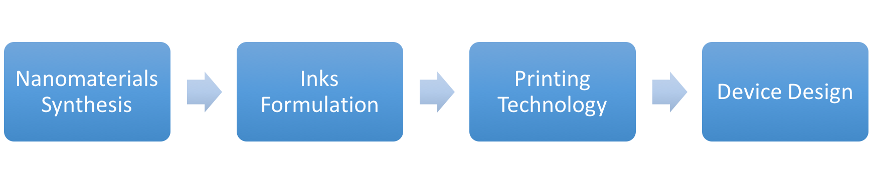
Vertical Integration key for Nanotechnology Products
Our proprietary technology allows for producing functional printed sensors in-house from the ground up. We make the semiconductor nanomaterials, functionalize and transfer them into inks. For best results we individually optimize the printing parameters for each ink. From the semiconductor nanomaterials to the final devices, we control every step of the process.
Nanomaterials Synthesis: Scalable Production of Semiconductor Nanowires
- US Nano’s patented process allows the large scale production of inorganic semiconductor nanowires
- Method dramatically lowers cost of nanowire synthesis compared to conventional batch methods
- Process can easily be modified to produce any type of semiconductor nanowire: III-V (e.g. InAs, GaAs) , IV (e.g. Si, Ge), II-VI (e.g. CdSe, CdS, ZnSe, CdTe, CdS, ZnO), and IV-VI (e.g. PbS, PbSe, ternary blends)
Nanoinks & Inkjet Printing of Nanomaterials
- Use of additive manufacturing addresses multiple problems associated with current subtractive semiconductor processing technologies, including dramatic waste reduction.
- Printing semiconductor nanowire devices does not require the tremendous set-up costs needed for wafer processing facilities.
- Flexibility in choice of semiconductor. Substituting a different semiconductor nanomaterial does not require any major changes in the manufacturing process (such as opening another super expensive semiconductor foundry) – it becomes just a different ink used in the device printing process.
Please visit our nanoinks & printing page to learn more.
Printed Electronics Device Design
- Essentially any size and shape semiconductor devices can be produced
- Cheap to produce various prototypes
- Easily to retool run to modify device design
- Production method is scalable, allowing for similar tools to be used from prototype to products
- Many different types of electronic devices can be manufactured
What are Semiconductor Nanowires?
All electronics require 3 elements: metals, semiconductors, and insulators. In nanotechnology, materials like conductive polymers or silver nanowires function as the metal element. There are fewer semiconductor nanomaterials available. At US Nano we have focused on developing inorganic nanowires as a cutting edge semiconductive nanomaterial. Nanowires are a one-dimensional material (length is much greater than diameter) meaning they have a high surface area to volume ratio. Additionally, Nanowires have both a macroscale (length) and a nanoscale (diameter) dimension. The nanoscale dimension can be used to tune properties through quantum effects, while the macroscale dimension can lead to rapid electron transport. This hybrid nature allows nanowires to have the “best of both worlds”. This is predicted to lead to dramatically better device performance relative to other semiconductive nanomaterials such as quantum dots. All these features combine to make nanowires attractive materials for nanotechnology.