US Nano’s scalable synthesis of nanowires is protected by US Patent 9,306,110. Additional patent applications pending in the United States and worldwide.
Summary of US Nano’s Nanomaterials Synthesis: Scalable Production of Semiconductor Nanowires
US Nano’s patented process allows the large scale production of inorganic semiconductor nanowires
process can run unattended for a day
produces gram quantities
product quality the same over the course of the run
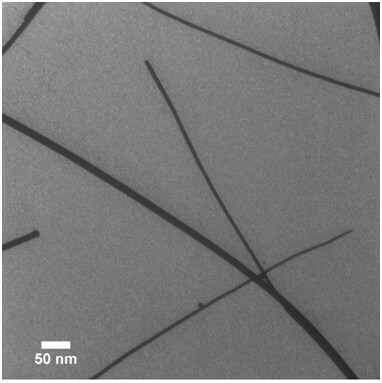
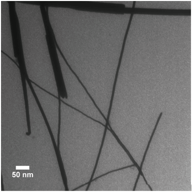
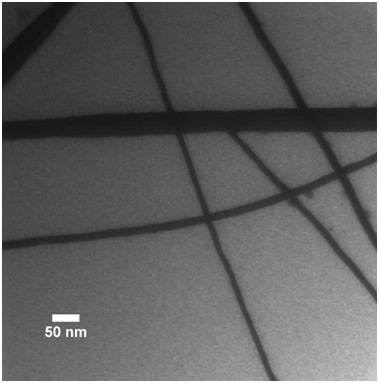
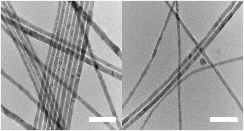
TEMs of the output of scalable synthesis of nanowires by hour. The images show the quality of nanowires produced hourly over a 9 hour CdSe Nanowire production run.
Methods lower synthesis dramatically
material costs into scalable commercialization ranges
further cost reduction opportunities still possible
Process can easily be modified to produce any type of semiconductor nanowire
III-V (e.g. InAs, GaAs)
IV (e.g. Si, Ge)
II-VI (e.g. CdSe, CdS, ZnSe, CdTe, CdS, ZnO)
IV-VI (e.g. PbS, PbSe, ternary blends)
core/shell wires (e.g. CdSe/ZnS)
If our method for the scalable synthesis of nanowires could accelerate your research or commercialization project, please contact us to discuss how we can help you.
Scalable Synthesis of Nanowires- US Nano’s Image Gallery
US Nano’s nanowire synthesis method can be used to produce large volumes of high quality nanowires. Some transmission electron micrographs (TEMs) of nanowires we’ve produced can be seen below. The nanowires can then be incorporated into nanoinks, and used to make various devices. Visit our technology page for an overview of the entire device fabrication process from start to finish.
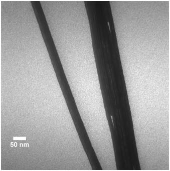
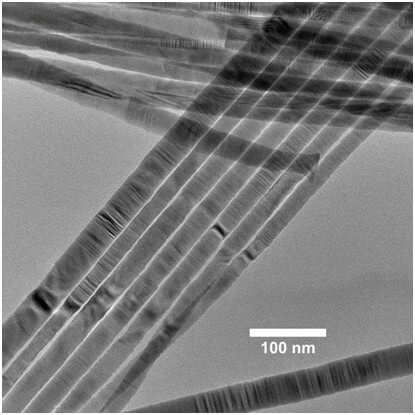
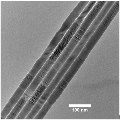
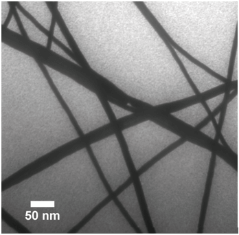
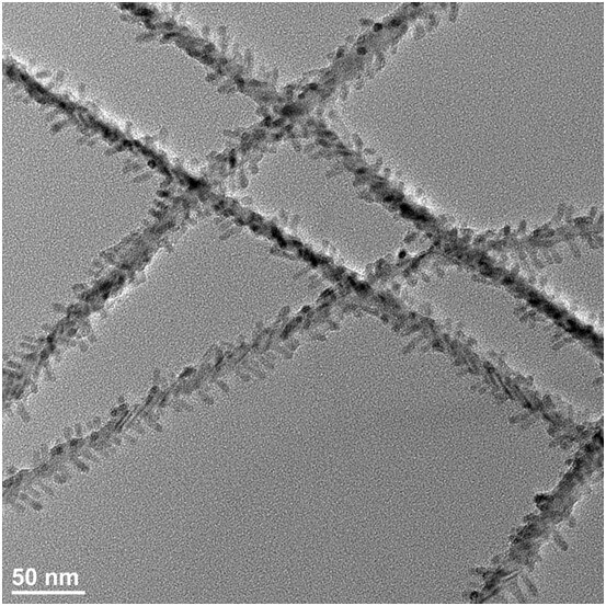
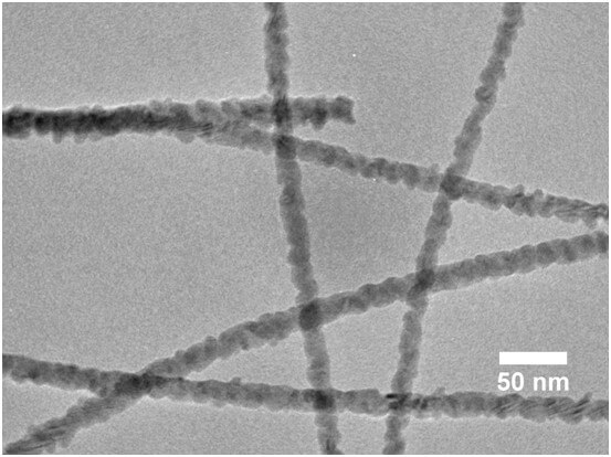
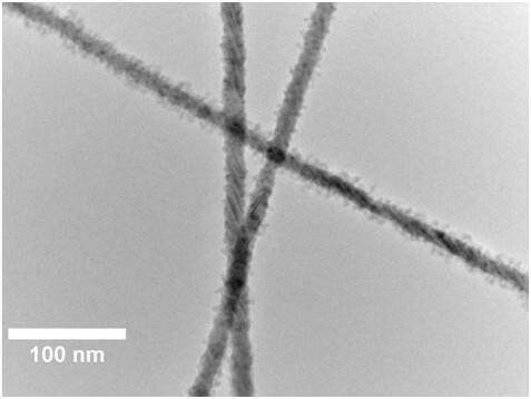
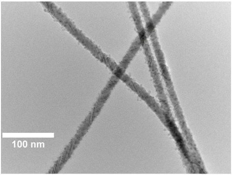
TEM image of the PbSe nanowires synthesized according to US Nano’s scalable synthetic method. The nanowires have an average diameter of 11.45 nm.Another TEM image of the PbSe nanowires synthesized according to US Nano’s scalable synthetic method. PbSe can be used for near infrared photosensing.Micrograph of CdSe Nanowires produced by US Nano’s process. The image shows both single wires and bundles of several wires.TEM of CdSe Nanowires showing a close-up of bundled CdSe Nanowires. A high degree of bundling tends to indicate smooth and long nanowires.TEM of high quality CdSe Nanowires produced by the US Nano method. The surface of these nanowires is extremely smooth.High resolution micrograph of a bundle of five CdSe nanowires. Smooth nanowires tend to self-assemble into bundles more.TEM of a network of CdSe Nanowires. High surface area chemical or biological sensors can be made from such a network of nanowires.TEM of 12 nm CdSe Nanowires produced using US Nano’s methods.A high surface area CdSe-CdS core-shell nanowire produced using US Nano’s patented process. The shell material, CdS, produces spiky nanorods on the surface of the nanowire.TEM of CdSe-CdS core-shell nanowires exhibiting a smoother shell. Nanowires were produced using US Nano’s patented process of nanowire synthesis.CdSe-ZnS Nanowires produced by US Nano’s scalable synthesis process. This CdSe-ZnS material could be used for photocatalytic applications.TEM of CdSe-ZnS core-shell nanowire produced by US Nano’s proprietary production method. Reaction conditions can be varied to tune the shell morphology.
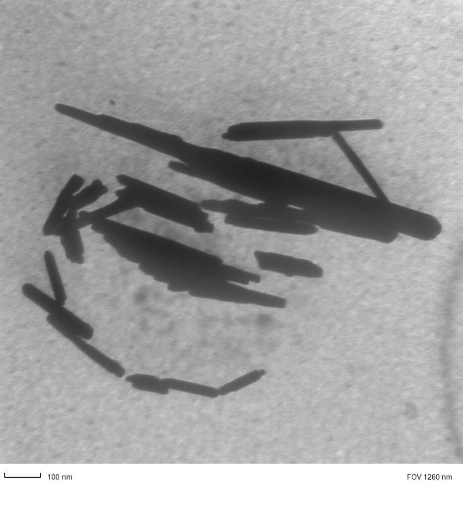
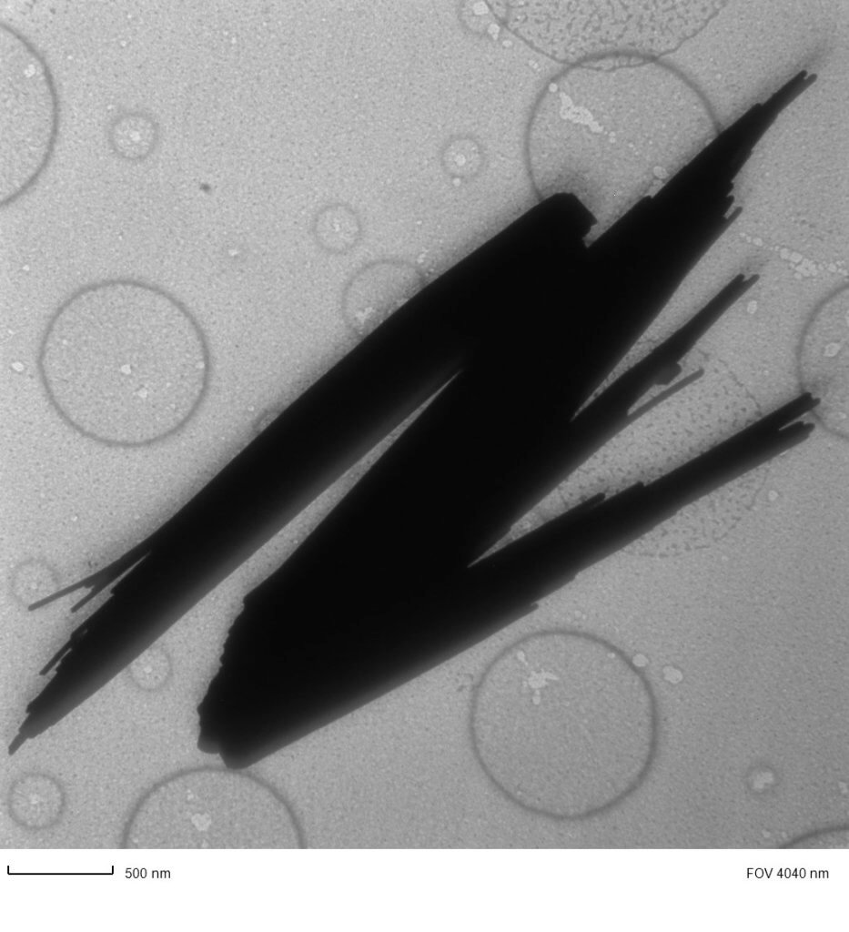
ZnO nanorods produced using US Nano’s synthetic process.Many ZnO Nanowires in a bundle.TEM of 1-2 micron ZnO nanowires.