
Nanowire based Flexible Electronics
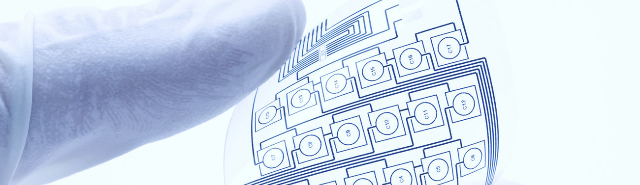
Inorganic semiconducting nanowires are an integral component to the expanding fields of printed and flexible electronics. This importance results from their semiconducting and electrical properties. Semiconducting nanomaterials can easily be incorporated in a variety of different manufacturing methods, such as inkjet and reel to reel printing.
Flexible materials can be used to make conformal electronics that could be stuck to skin, fabric, walls or windows. The solution-based nature of flexible electronic manufacturing makes fabrication costs dramatically cheaper than a lithographic fabrication and allows for the large scale. Flexible/printed electronics technology is expected to be applied to a variety of applications including energy (photovoltaics, batteries, and lighting), consumer devices (displays, sensors, and actuators), healthcare (sensors), communication (RFID), and defense (sensors, photovoltaics, displays). The area of flexible/printed electronics is a rapidly growing market, with experts predicting its size to be $250 billion dollars by 2025.
Many different flexible electronic products are already available on the market or are currently in research and development. Organic photovoltaic’s (OPV’s) are expected to become widely available, and eventually transition to building integrated PV’s. Electric property limitations of organic electronics suggest inorganic nanowire flexible electronics may be suitable replacements in the near future. Flexible displays are currently being created for all applications, including home entertainment use (1). Organic light-emitting diode (OLED) lighting is already available and is expected to become a huge commercial product (1). Various other flexible electronics also being integrated into the market include printed logic circuits (2), flexible batteries, radio frequency identification (RFID) (3) and single-crystal nanowire transistors (4). The flexible form factor is also critical for the next generation of wearable electronics.
Selected Literature on Nanowire based Flexible Electronics
Several procedures have been published detailing the assembly of nanowires for use in flexible electronic devices, including the ability to assemble on plastic or other flexible substrates.
Mechanical Methods of Nanowire Assembly
Lieber, Yu and Cao produced blown bubble films (popular in the polymer industry) with bubble walls containing nanowires. The bubble film was then used to uniformly transfer nanowires to both flexible and curved surfaces in addition to traditional rigid substrate. They were able to use this technique to fabricate multiple nanowire field-effect transistors (FET). Creating bubbles with larger diameters would enable the transfer of nanowires to very large surfaces (10).
Fluidics can also be used to assemble nanowires into functional networks. Lieber, Huang, Duan and Wei created a channel on substrate with a PDMS mold, and flowed nanowires to create a parallel array. Alternating flow directions resulted in crossed arrays. They demonstrated the ability to make nanoscale devices by testing a 2 by 2 crossbar array made from n-type InP nanowires; the current-voltage data observed was the expected result for an n-n type junction (9).
Korgel and coworkers have found that nanowires possess a very high strength-to-weight ratio and have investigated the stress and elastic properties of nanowires. They then used vacuum filtration to create a flexible, non-woven fabric made from germanium nanowires (8).
Electrical Methods of Nanowire Assembly
Nanowires are frequently assembled into various devices or fibers using electric fields. Gates and coworkers were also able to assemble macroscopic fiber made from nanomaterial. They used electrokinetic techniques to organize nanowires in solution into fibers; these fibers can then be separated from the solution (11).
Petchsang, McDonald, Sinks and Kuno have used light induced nanowire assembly (LINA) to assemble macroscopic CdSe nanowire yarns. Photoexcitation allows nanowires to be aligned into these macroscopic structures while still retaining their useful optical and electrical properties (12). You can create solar thread with this technique, which is an interesting example of a flexible electronic device.
Similarly, Freer and coworkers used dielectrophoretic nanowire assembly to integrate the bottom-up assembly of nanowires with well developed top-down lithography techniques, exhibiting control over nanowire alignment and position (4). Chang, Kuno, Xing and coworkers also used dielectrophoresis to align CdSe nanowires. Super-band-gap illumination enhances the conductivity of the wires, thus increasing the induced dipole. This consequently decreases the assembly time (13). Drndić and coworkers used electrodes to create electric fields capable of adjusting the location and direction of CdSe nanorods after being drop-cast from a solution (14).
Enable your Flexible Electronics research with US Nanotechnology
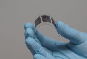 US Nano has intellectual property relating to the industrial scale synthesis of semiconductor nanowires available for licensing or joint development opportunities. The company also has methods formulate these nanowires into inks suitable for inkjet printing nanowires. Additionally, US Nano has developed methods to inkjet print nanowires, allowing for the rapid production of fast, cheap, and rugged flexible electronic devices such as nanowire based photosensors. An overview of our skills across the entire device fabrication process can be found on our Technology page.
Contact us to discuss how we can advance your energy research through licensing or joint development projects.
Selected References on Flexible Electronics
- OE-A Roadmap for Organic and Printed Electronics. Organic Electronics 2011.
- Whang, D.; Jin, S.; Lieber, C. M. Large-Scale Hierarchical Organization of Nanowires for Functional Nanosystems. Japanese Journal of Applied Physics 2004, 43, 4465–4470.
- Fan, Z.; Ho, J. C.; Takahashi, T.; Yerushalmi, R.; Takei, K.; Ford, A. C.; Chueh, Y.-L.; Javey, A. Toward the Development of Printable Nanowire Electronics and Sensors. Advanced Materials 2009, 21, 3730–3743.
- Freer, E. M.; Grachev, O.; Duan, X.; Martin, S.; Stumbo, D. P. High-yield self-limiting single-nanowire assembly with dielectrophoresis. Nature Nanotechnology 2010, 5, 525–30.
- Li, Z.; Ma, X.; Sun, Q.; Wang, Z.; Liu, J.; Zhu, Z.; Qiao, S. Z.; Smith, S. C.; Lu, G. M.; Mews, A. Synthesis and Characterization of Colloidal Core-Shell Semiconductor Nanowires. European Journal of Inorganic Chemistry 2010, 2010, 4325–4331.
- Lange, H.; Mohr, M.; Artemyev, M.; Woggon, U.; Niermann, T.; Thomsen, C. Optical phonons in colloidal CdSe nanorods. Physica Status Solidi (B) 2010, 247, 2488–2497.
- Abe, S.; Čapek, R. K.; De Geyter, B.; Hens, Z. Tuning the postfocused size of colloidal nanocrystals by the reaction rate: from theory to application. ACS Nano 2012, 6, 42–53.
- Smith, D. A.; Holmberg, V. C.; Korgel, B. A. Flexible germanium nanowires: ideal strength, room temperature plasticity, and bendable semiconductor fabric. ACS Nano 2010, 4, 2356–62.
- Huang, Y.; Duan, X.; Wei, Q.; Lieber, C. M. Directed assembly of one-dimensional nanostructures into functional networks. Science 2001, 291, 630–3.
- Yu, G.; Cao, A.; Lieber, C. M. Large-area blown bubble films of aligned nanowires and carbon nanotubes. Nature Nanotechnology 2007, 2, 372–7.
- Wang, M. C. P.; Zhang, X.; Majidi, E.; Nedelec, K.; Gates, B. D. Electrokinetic Assembly of Selenium and Silver Nanowires into Macroscopic Fibers. ACS Nano 2010, 4, 2607–2614.
- Petchsang, N.; Mcdonald, M. P.; Sinks, L. E.; Kuno, M. Light Induced Nanowire Assembly : The Electrostatic Alignment of Semiconductor Nanowires into Functional Macroscopic Yarns. Advanced Materials 2012, 1–5.
- Zhou, R.; Chang, H.; Protasenko, V.; Kuno, M.; Singh, A. K.; Jena, D.; (Grace) Xing, H. CdSe nanowires with illumination-enhanced conductivity: Induced dipoles, dielectrophoretic assembly, and field-sensitive emission. Journal of Applied Physics 2007, 101, 073704.
- Hu, Z.; Fischbein, M. D.; Querner, C.; Drndić, M. Electric-field-driven accumulation and alignment of CdSe and CdTe nanorods in nanoscale devices. Nano Letters 2006, 6, 2585–91.