
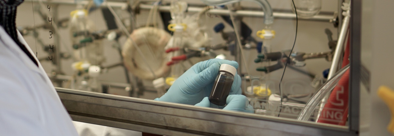
Formulation of Semiconductor Nanoinks
Formulation of nanowire inks (“nanoinks”) is a critical our workflow. Importantly, the ink that comes out of this step is semiconductor agnostic-a CdSe ink is just as printable as a ZnO ink. If ink formulation is done properly, no other step downstream should care about the nature of the semiconductor nanowire. This allows us incredible flexibility in device design and production.
Nanoink formulation has two main goals: to produce an ink that is ink-jettable and to produce an ink with advanced functionality. As we modify the surface ligands (molecules) on the nanowires we can provide handles to, for example, covalently attach an antibody to the nanowire. We may use a mixture of ligands on a given nanowire; this improves solubility, stability, jettability, or sensing.
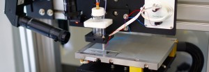
Inkjet Printing of Nanowires
Printing allows the production of devices in high volumes, on large areas, and for low costs. Printing enables the creation of devices on a variety of substrates, including flexible films such as plastics and metal foils, in addition to conventional rigid substrates such as glass or semiconductor wafers. For more information about flexible electronics, please visit our Flexible Electronics page.
Inkjet printing allows for a wide range of feature sizes to be printed, ranging from ~100 microns to many square centimeters. This allows us flexibility in device design, though inkjet is a slow printing technology. Inkjet is also a “drop-on-demand” technology, allowing for minimal waste of expensive R&D materials. Inkjet is a well-established printing process, and a variety of commercial vendors produce manufacturing grade printers. However, translation of our nanowire inks to high-throughput/ roll-to-roll can also be performed once the prototyping in completed.
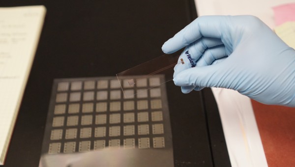
Fabrication of Devices via Inkjet Printing
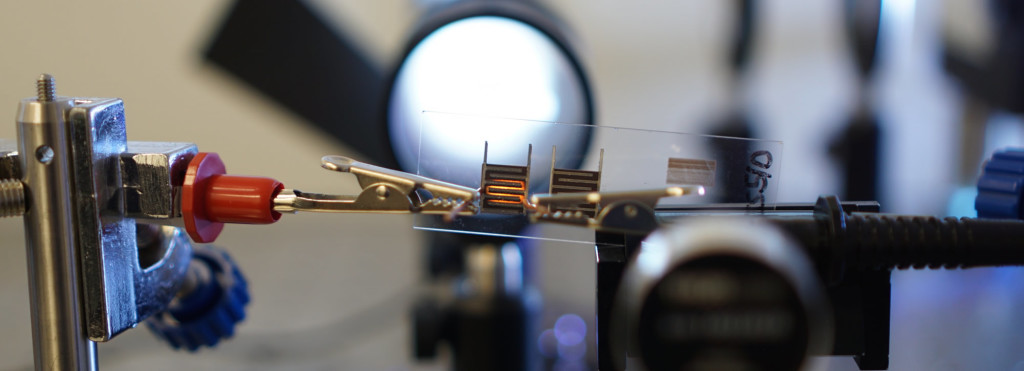
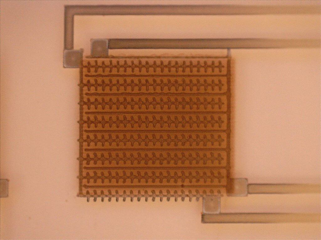
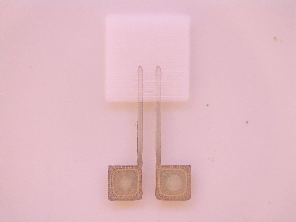
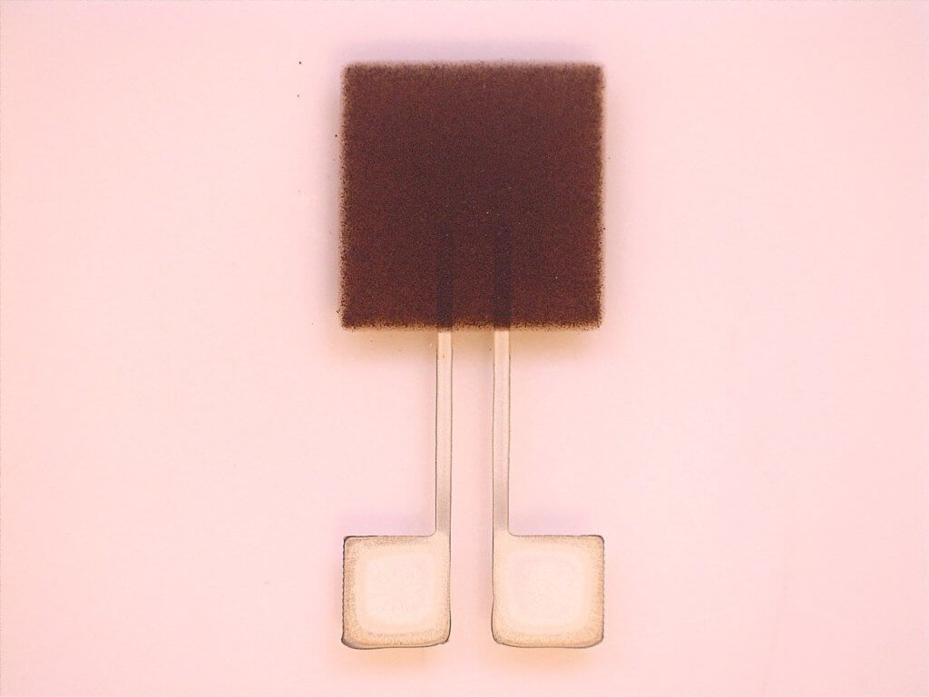
We can print the electrodes, the semiconductor pad, and a well to contain the fluid sample. This allows us to rapidly explore how different design parameters (sensing area, volume of sample, etc.) impact the device performance. In a manufacturing setting, it is likely that the entire device would not be built from inkjet printing, but for R&D it allows us to make precisely modified prototypes rapidly.
We have printed photosensors, photovoltaics, TFTs, chemical and biological sensors. Inkjet printing allows us to print an entire device from the bottom up.
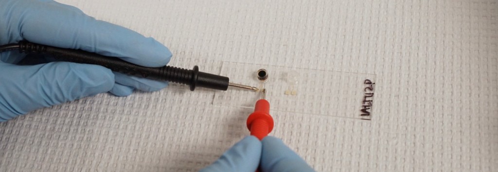
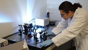
Examining the printed electrodes for defects.

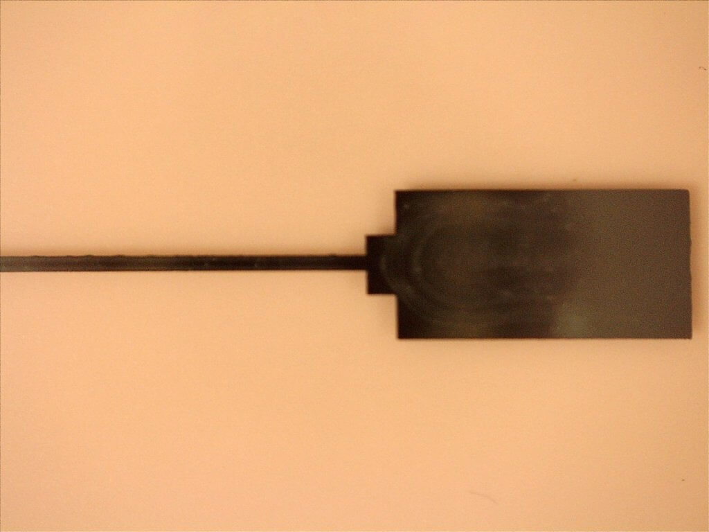
A fully printed chemical nanosensor requires a well to hold the analyte. Capacity testing of polyimide based wells. Well overflows at 50 µL of buffer.


If you think our printing expertise could help your printed electronics project, please contact us.